# What is a Hardware Description Language (HDL)
In the early days of digital electronics, [digital circuits](How%20FPGA%20works.md#Digital-circuits) drawn on paper were small, while their physical hardware implementations were large. As electronics evolved into microelectronics, the paper diagrams grew increasingly complex, while the physical size of their chip implementations shrank dramatically. In _Fig. 1_, you can see the digital circuit of the Intel 4004 processor, released in 1971.
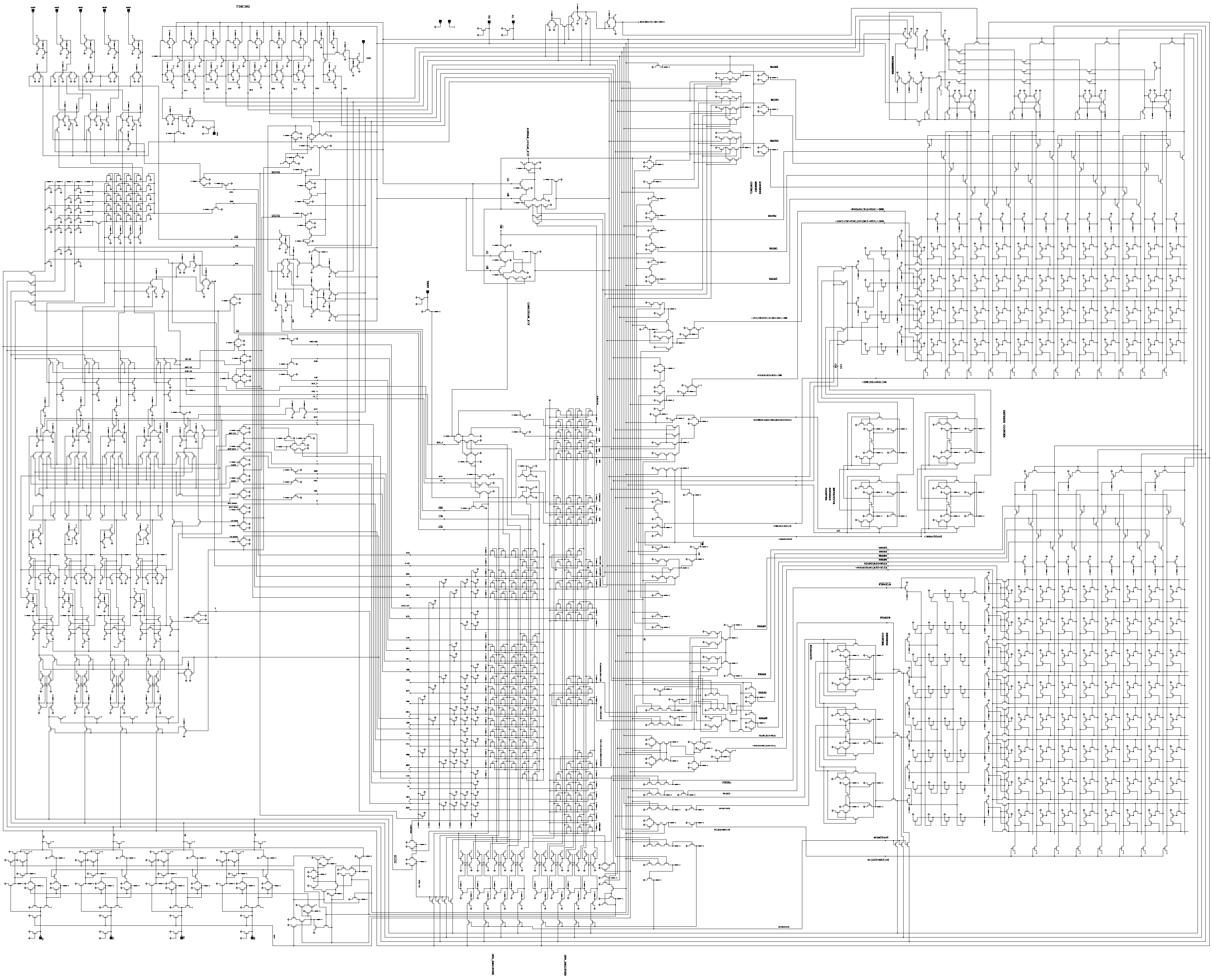
_Figure 1. Digital circuit of the Intel 4004 processor at the transistor level [[1]](https://www.4004.com/mcs4-masks-schematics-sim.html)._
This chip contains 2,300 transistors [[2]](https://en.wikipedia.org/wiki/Intel_4004).
Over the past fifty years, the complexity of digital circuits has grown enormously. Modern desktop processors contain tens of billions of transistors. If printed at its original scale, the diagram above would occupy a rectangle of 115×140 cm, with an area of about 1.6 m2. Assuming that the print area scales linearly with the transistor count, printing the circuit of a modern processor with 23 billion transistors would require an area of 16 million m2 — equivalent to a square with a side length of 4 km.
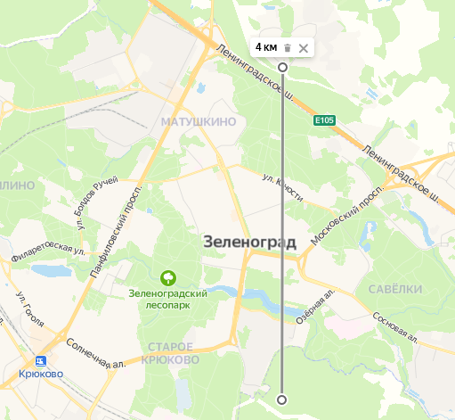 _Figure 2. The scale that digital circuit diagrams of modern processors would reach if printed on paper._
As you might guess, at some point between 1971 and 2024, engineers stopped designing digital circuits by drawing them on paper.
Of course, when designing a device, it is not necessary to draw every transistor on a schematic — complexity can be managed by moving between levels of abstraction. For example, one can start designing at the level of functional blocks, and then draw the schematic for each individual block.
For instance, the Intel 4004 circuit can be represented as follows:
_Figure 2. The scale that digital circuit diagrams of modern processors would reach if printed on paper._
As you might guess, at some point between 1971 and 2024, engineers stopped designing digital circuits by drawing them on paper.
Of course, when designing a device, it is not necessary to draw every transistor on a schematic — complexity can be managed by moving between levels of abstraction. For example, one can start designing at the level of functional blocks, and then draw the schematic for each individual block.
For instance, the Intel 4004 circuit can be represented as follows:
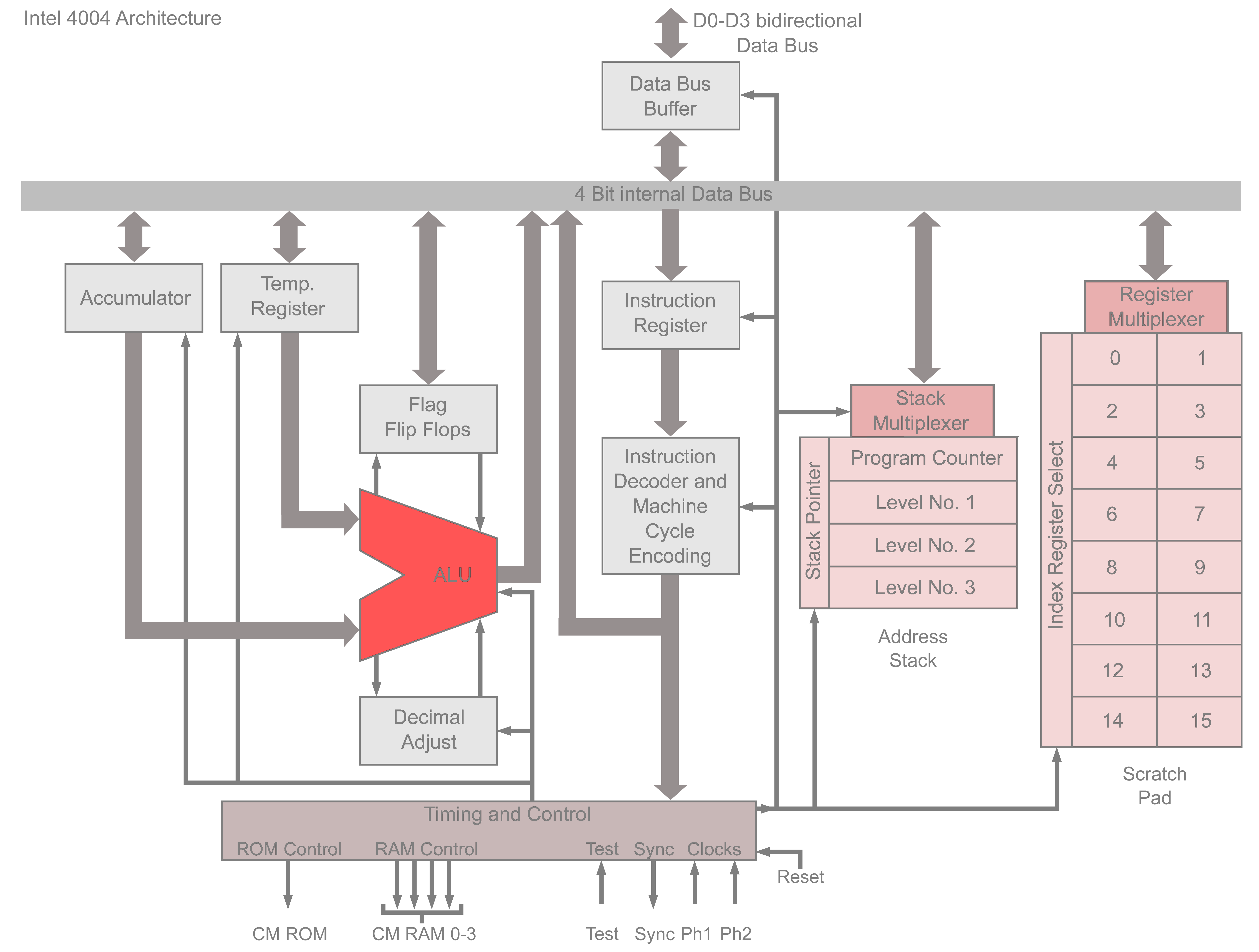 _Figure 3. Digital circuit of the Intel 4004 processor at the functional block level [[2]](https://en.wikipedia.org/wiki/Intel_4004)._
However, even individual blocks can sometimes be quite complex. Consider the hardware AES encryption block [[3]](https://csrc.nist.gov/files/pubs/fips/197/final/docs/fips-197.pdf) shown in Figure 4:
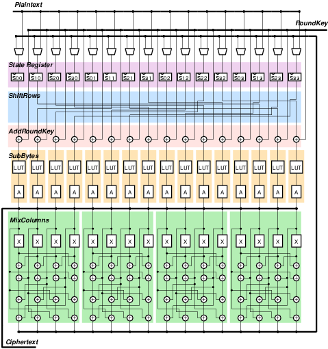
_Figure 4. Digital circuit of a hardware AES encryption block [[4]](https://iis-people.ee.ethz.ch/~kgf/acacia/acacia_thesis.pdf)._
Note that even this block is not shown at the individual transistor level. Each XOR operation, multiplication, signal multiplexing, and substitution table is a separate block whose functionality still needs to be implemented.
At some point, engineers realized it was simpler to describe a digital circuit in textual form rather than graphical form.
How can a digital circuit be described in text? Let us consider the digital circuit of a half-adder:

_Figure 5. Digital circuit of a half-adder at the logic gate level._
This **module** (_half-adder_) has two **inputs**: _a_ and _b_, and two **outputs**: _sum_ and _carry_.
The _sum_ output is the **result** of the logical **XOR** operation on operands _a_ and _b_.
The _carry_ output is the **result** of the logical **AND** operation on operands _a_ and _b_.
The text above is precisely the description from which this digital circuit can be reconstructed. If the description is standardized, only the words in bold and italics need to be retained. The following is an example of how this circuit could be described according to the IEEE 1364-2005 standard (the Verilog Hardware Description Language — HDL):
```Verilog
module half_sum( // module half-adder with
input a, // input a,
input b, // input b,
output sum, // output sum and
output carry // output carry.
);
assign sum = a ^ b; // Where output sum is the result of XOR of a and b,
assign carry = a & b; // and output carry is the result of logical AND of a and b.
endmodule
```
At first glance, this description appears even longer than the natural-language version. However, the extra length comes only from line breaks and some redundancy in the port declarations, which was added to improve readability. The same description could also be written as:
```Verilog
module half_sum(input a, b, output sum, carry);
assign sum = a ^ b;
assign carry = a & b;
endmodule
```
It is important to note that Verilog code describes the device as a whole, all at once. It's a **description of a circuit**, not **line-by-line program execution**.
With practice, describing a circuit in text becomes much easier and requires no graphical representation. A specification — a formal statement of how the device should behave — is sufficient. From it, an algorithm is developed, which is then expressed as an HDL description.
An interesting fact: it was mentioned earlier that engineers stopped designing devices by drawing digital circuits sometime between 1971 and 2024. The first conference dedicated to hardware description languages was held in 1973 [[5, p. 8]](https://dl.acm.org/doi/pdf/10.1145/3386337). Thus, the Intel 4004 can be considered one of the last digital devices designed without the use of hardware description languages.
## References
1. [Intel 4004 — 50th Anniversary Project](https://www.4004.com/mcs4-masks-schematics-sim.html);
2. [Wikipedia page on Intel 4004](https://en.wikipedia.org/wiki/Intel_4004);
3. [F. Kağan Gürkaynak / Side Channel Attack Secure Cryptographic Accelerators](https://iis-people.ee.ethz.ch/~kgf/acacia/acacia_thesis.pdf);
4. [FIPS 197, Advanced Encryption Standard (AES)](https://csrc.nist.gov/files/pubs/fips/197/final/docs/fips-197.pdf);
5. [P. Flake, P. Moorby, S. Golson, A. Salz, S. Davidmann / Verilog HDL and Its Ancestors and Descendants](https://dl.acm.org/doi/pdf/10.1145/3386337).
_Figure 3. Digital circuit of the Intel 4004 processor at the functional block level [[2]](https://en.wikipedia.org/wiki/Intel_4004)._
However, even individual blocks can sometimes be quite complex. Consider the hardware AES encryption block [[3]](https://csrc.nist.gov/files/pubs/fips/197/final/docs/fips-197.pdf) shown in Figure 4:

_Figure 4. Digital circuit of a hardware AES encryption block [[4]](https://iis-people.ee.ethz.ch/~kgf/acacia/acacia_thesis.pdf)._
Note that even this block is not shown at the individual transistor level. Each XOR operation, multiplication, signal multiplexing, and substitution table is a separate block whose functionality still needs to be implemented.
At some point, engineers realized it was simpler to describe a digital circuit in textual form rather than graphical form.
How can a digital circuit be described in text? Let us consider the digital circuit of a half-adder:

_Figure 5. Digital circuit of a half-adder at the logic gate level._
This **module** (_half-adder_) has two **inputs**: _a_ and _b_, and two **outputs**: _sum_ and _carry_.
The _sum_ output is the **result** of the logical **XOR** operation on operands _a_ and _b_.
The _carry_ output is the **result** of the logical **AND** operation on operands _a_ and _b_.
The text above is precisely the description from which this digital circuit can be reconstructed. If the description is standardized, only the words in bold and italics need to be retained. The following is an example of how this circuit could be described according to the IEEE 1364-2005 standard (the Verilog Hardware Description Language — HDL):
```Verilog
module half_sum( // module half-adder with
input a, // input a,
input b, // input b,
output sum, // output sum and
output carry // output carry.
);
assign sum = a ^ b; // Where output sum is the result of XOR of a and b,
assign carry = a & b; // and output carry is the result of logical AND of a and b.
endmodule
```
At first glance, this description appears even longer than the natural-language version. However, the extra length comes only from line breaks and some redundancy in the port declarations, which was added to improve readability. The same description could also be written as:
```Verilog
module half_sum(input a, b, output sum, carry);
assign sum = a ^ b;
assign carry = a & b;
endmodule
```
It is important to note that Verilog code describes the device as a whole, all at once. It's a **description of a circuit**, not **line-by-line program execution**.
With practice, describing a circuit in text becomes much easier and requires no graphical representation. A specification — a formal statement of how the device should behave — is sufficient. From it, an algorithm is developed, which is then expressed as an HDL description.
An interesting fact: it was mentioned earlier that engineers stopped designing devices by drawing digital circuits sometime between 1971 and 2024. The first conference dedicated to hardware description languages was held in 1973 [[5, p. 8]](https://dl.acm.org/doi/pdf/10.1145/3386337). Thus, the Intel 4004 can be considered one of the last digital devices designed without the use of hardware description languages.
## References
1. [Intel 4004 — 50th Anniversary Project](https://www.4004.com/mcs4-masks-schematics-sim.html);
2. [Wikipedia page on Intel 4004](https://en.wikipedia.org/wiki/Intel_4004);
3. [F. Kağan Gürkaynak / Side Channel Attack Secure Cryptographic Accelerators](https://iis-people.ee.ethz.ch/~kgf/acacia/acacia_thesis.pdf);
4. [FIPS 197, Advanced Encryption Standard (AES)](https://csrc.nist.gov/files/pubs/fips/197/final/docs/fips-197.pdf);
5. [P. Flake, P. Moorby, S. Golson, A. Salz, S. Davidmann / Verilog HDL and Its Ancestors and Descendants](https://dl.acm.org/doi/pdf/10.1145/3386337).